
Hitachi SU8010 Cold Field Emission SEM Location: Room 181, IPST Bldg
- Please contact Tim Zhang for training
- 1.0 nm resolution( Secondary electron detector) at 15 kV and 1.3 nm at 1 kV
- 2.0nm resolution(Backscattered electron detector) at 15KV
- Operating voltage range 100 V – 30 kV
- High resolution image grabber up to 5120X3840 pixels.
- Ultra-clean vacuum system with a turbo pump and an oil free dry-scroll pump.
- A stationary anti-contamination trap reduce the re-deposition of hydrocarbons onto the sample surface
- Operating Instructions

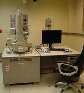
LEO 1530 thermally-assisted field emission (TFE) scanning electron microscope (SEM)
Location: room 176, IPST Bldg.
- State-of-the-art; 1 nm resolution at 20 kV and 3 nm at 1 kV operating voltage range 200 V – 30 kV
- large specimen chamber and eucentric stage
thin window SSD energy dispersive spectrometer (EDS), for microanalysis of elements down to Boron. - – Operating Instructions