Silicon photomultipliers (SiPM) have been attracting many interests in several application fields since its early development stage [1]. Operating with scintillators, SiPM has become very active in the investigation area of nuclear instruments and methods as an alternative to photomultiplier tube (PMT) to detect light with very low intensity , due to its several advantages, i.e., low operation voltage, low power consumption, withstanding to magnetic field, compactness, ruggedness and low cost [2]. Very promising and gradual progresses in SiPM performance have also been made recently. However, the peak value of photo-detection efficiency (PDE) of SiPM device is still limited to around 50%. Among the efficiency limiting factors (including avalanche triggering probability and geometrical fill factor), quantum efficiency is an important one as it is related to photon absorption, generation of a primary electron-hole pair in the active volume, and carrier collection (photo-generated primary carriers travel to the high-field region). Therefore, we study an excellent surface passivation enabled by an ultrathin Al2O3 film that is synthesized by plasma-assisted atomic layer deposition (ALD) to reduce carrier recombination on the active area surface and thus improve quantum efficiency in the short wavelength range. The superiority of Al2O3 passivation on p+ surfaces is due to a high density (on the order of 1013 cm-2) of built-in negative charges, which might be present at the tetrahedrally coordinated Al site at the interface, in contrast to the octahedrally coordinated site where Al has a charge of 3+ [3]. For comparison purposes, thermal SiO2 and SiNx that are typically employed in SiPM devices for surface passivation are included in our research.
The studies of surface passivation on low resistivity n-type and p-type is also reviewed in our work, which can verify the feasibility of Al2O3 film on the surfaces of guard ring and trench isolation regions of SiPM device. Our investigation is process by integrating Al2O3 surface passivation into SiPM prototype device with p+/n–/n/n+ structure, as shown in Fig. 1.

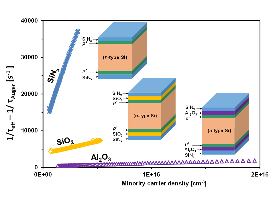
The passivation quality of Al2O3 film on p+ layer can be quantified by the emitter saturation current density (J0e), which is determined from quasi-steady-state photoconductance (QSSPC) characterization technique [4]. J0e is extracted from the slope of linear fit of the measured Auger-corrected inverse effective lifetime as a function of the injection level. Note that symmetric structure is required for tested samples in order to apply this characterization technique, i.e., SiNx/Al2O3/p+/c-Si/p+/Al2O3/SiNx, where SiNx works as an antireflective coating (ARC) layer, as shown in Fig. 2. Applying this characterization technique, the level of surface passivation can also be quantified by the upper limit of the effective surface recombination velocity (Seff), assuming an infinite bulk lifetime for the c-Si substrate [5].

- Sadygov, Russian Patent nr. 2086047 C1, 1997.
- Renker, “Geiger-mode avalanche photodiodes, history, properties and problems,” Nucl. Instrum. Meth. A, vol. 567, no. 1, pp. 48-56, Nov. 2006.
- S. Johnson, G. Lucovsky, and I. Baumvol, “Physical and electrical properties of noncrystalline Al2O3 prepared by remote plasma enhanced chemical vapor deposition,” J. Vac. Sci. Technol. A, vol. 19, no. 4, pp. 1353-1360, Jul./Aug. 2001.
- A. Sinton and A. Cuevas, “Contactless determination of current–voltage characteristics and minority‐carrier lifetimes in semiconductors from quasi‐steady‐state photoconductance data,” Appl. Phys. Lett., vol. 69, no. 17, pp. 2510-2512, Aug. 1996.
- Hoex, S.B.S. Heil, E. Langereis, M.C.M. van de Sanden, and W.M.M. Kessels, “Ultralow surface recombination of c-Si substrates passivated by plasma-assisted atomic layer deposited Al2O3,” Appl. Phys. Lett., vol. 89, no. 4, pp. 042112, Jul. 2006.
- Y. Tao, K. Madani, E. Cho, B. Rounsaville, V. Upadhyaya, and A. Rohatgi, “High-efficiency selective boron emitter formed by wet chemical etch-back for n-type screen-printed Si solar cells,” Appl. Phys. Lett., vol. 110, no. 2, pp. 201101, Jan. 2017.
- Y. Tao, and A. Rohatgi, “High-efficiency front junction n-type crystalline silicon solar cells,” in Nanostructured Solar Cells, 2017, ch. 5, pp. 93-115.
