SOP Substrate & Systems Integration Lab
This is a class 1,000 clean room facility maintained at 68F and relative humidity of 35%. This test bed and prototype research laboratory enables the processing of up to 300 mm substrates and interposers made of organics, glass, flex, ceramics, and silicon with dielectrics build up, via formation and metallization for high density wiring (HDW), and actives and passives embedding for heterogenous integration. Process capabilities in this laboratory include substrate cleaning and preparation, polymer deposition of wet films through spin coating, polymer deposition of dry films through roll or vacuum lamination, soft bake and final film curing, laser via drilling, full field photolithography for feature development, develop, etch and strip of resists and PIDs, feature inspection and characterization, both electrolytic and electroless copper plating for build-up, and gold, nickel and solder plating for surface finish. Equipment includes:
Advanced Assembly Technologies
Flip Chip Bonding
Systems within IEN support research projects needing flip chip assembly employing various bonding methods with fine pitch interconnections, moderate heating rates, and tight planarity control.
Fintech Lambda Manual Flip Chip Bonders (Pettit Cleanroom and Marcus Lab)
- Better than 1um placement accuracy
- Split vision system to enable intuitive chip to substrate alignment
- Substrate sizes up to 100mm wafer
- Inert or reducing atmosphere cover to enable nitrogen or forming gas blanketing of bonding area
- Side camera view to monitor chip touch-down and solder reflow
- Chip and substrate heating capabilities up to 6 degree per second to 400C max
- Custom tooling options for thin device handling and various chip sizes commonly .4mm to 60mm square.
- Bonding force from 0.1 N to 20 N
- Common technologies: Thermocompression bonding, Thermosonic bonding, reflow bonding, chip pickup, chip placement, rework.

Fintech Matrix Semi-Automatic Flip Chip Bonder (Pettit Cleanroom)
- Better than 3um placement accuracy
- Split vision system to enable intuitive chip to substrate alignment
- Substrate sizes up to 150mm square with some overhang
- Inert or reducing atmosphere cover to enable nitrogen, forming gas, or formic acid vapor blanketing of bonding area
- Side camera view to monitor chip touch-down and solder reflow
- Chip and substrate heating capabilities up to 6 degree per second to 400C max
- Custom tooling options for thin device handling and various chip sizes commonly .4mm to 100mm square.
- Bonding force from 0.1 N to 450 N with software controlled force application and ramping
- Common technologies: Thermocompression bonding, Thermosonic bonding, reflow bonding, chip pickup, chip placement, rework, panel assembly.

Fintech Lambda 2 Semi-Automatic Flip Chip Bonder (Marcus Lab)
- Better than 1um placement accuracy
- Split vision system to enable intuitive chip to substrate alignment
- Substrate sizes up to 40mm square
- Inert or reducing atmosphere cover to enable nitrogen, forming gas, or formic acid vapor blanketing of bonding area
- Side camera view to monitor chip touch-down and solder reflow
- Chip and substrate heating capabilities to 450C
- Custom tooling options for thin device handling and various chip sizes commonly .1mm to 20mm square
- Bonding force from 0.1 N to 400 N
- Semiautomated pneumatic dispense capability for uv-curable materials or underfills
- UV cure capability
- Common technologies: Thermocompression bonding, Thermosonic bonding, reflow bonding, chip pickup, chip placement, rework.

Wirebonding
Systems within IEN support research projects needing wirebonding capabilities for high power devices, MEMS devices, packaging of sensitive electronics for consolidation into larger systems and test fixtures, and single sided fabricated devices without the need for TSV’s.
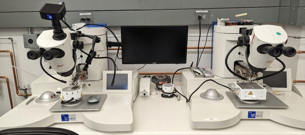
TPT HB16 Wirebonders (Pettit Lab)
- Aluminum wedge and gold ball bonding
- Camera system and alignment assistance pointer for easy manual alignment of bonds
- Substrate sizes up to 100mm square on heated stage
- Pad dimensions commonly 100um minimum
- Wire size commonly 25um aluminum and 25um gold
- Manual, semiautomatic and limited programmable bonding placement with motorized y stage
- Options for ribbon wedge bonding up to 250x25um ribbon size
- Options for copper wirebonding with forming gas accessory (proposed)
- Intuitive touchscreen control for process setup and multi mouse operation
- Motorized 2 inch spool and manual 1/2 inch spool options
- Common technologies: Ball bonding, wedge bonding, stud bumping, ribbon wedge bonding
Solder Reflow
Systems within IEN support research projects needing solder reflow processing with a nitrogen atmosphere to reduce oxidation of assemblies with moderate heating rates tailored to lead free reflow.
LPKF Protoflo S (Pettit Cleanroom)
- Computer controlled reflow processing
- Nitrogen atmosphere available for oxide formation mitigation
- Motorized drawer system with window for easy loading and monitoring of sample status
- Maximum reflow temperature 320C
- 9inch by 12inch substrate size capability
- Real time monitoring up to 4 extra thermocouple inputs in addition to internal measurement

Inspection
Systems within IEN support research projects needing packaging-oriented inspection and metrology. Supplementing a wider collection of inspection capabiltiies within IEN.
Dage X-Ray (Pettit Lab)
- 0.75 um feature recognition capability
- Up to 70 degree off angle viewing
- Automated inspection routine capabilities
- Numerous image enhancement capabilities related to edge detection and filtering
- Multiple image overlay for sharpening of image
- Large work area can handle substrate up to 22 inch dimension

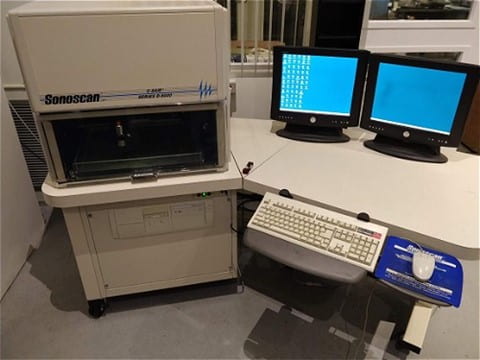
Sonoscan SAM D9000 (Pettit Lab)
- Differential scan of interfaces between layers to characterize delamination
- 12 inch working stage area for image immersed in DI water
- Resolution down to a few microns
- Reflected and transmission scan capability up to 230MHz
- Computer control and selectable color maps to highlight specific defects
Akrometrix Shadow Moire PS200S (Pettit Lab)
- 150mm x 200mm substrate max capability
- Approximately 3um resolution across substrate
- Automated measurement of warpage of substrates at room temperature and throughout a heating process
- Substrates must be uniform color and can be temprorarily painted or coated to enable characterization
- Sample tracking allows measurement of multiple parts at one time.
- Interface analysis capability to characterize the gap change between two devices when digitally stacked together

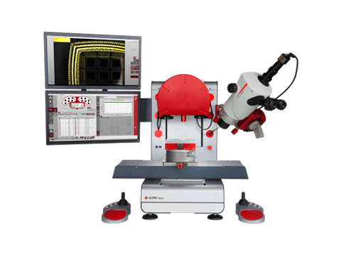
Xyztec Condor Sigma Bond Tester (Pettit Cleanroom)
- Die shear capability up to 200kg of force application and interchangeable tool heads
- Wire pull, die shear, ball shear, tweezer pull capabilities
- Automated data collection for destructive or non-destructive testing
- Touch and rebound shear height setting option
- Automatic shearing of multiple devices in a row option
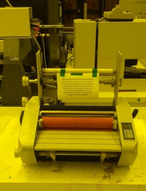
Lamination Tools (Dry Films, Dielectric, Photoresists)


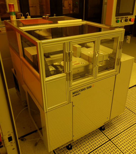
Meiki Vacuum Laminator (MVLP300)
- Good results over old Hi-Vac system
- 300mm substrate capacity
- 180 C max temperature
- 1 MPa max pressure to act as a vacuum laminator and vacuum hot press
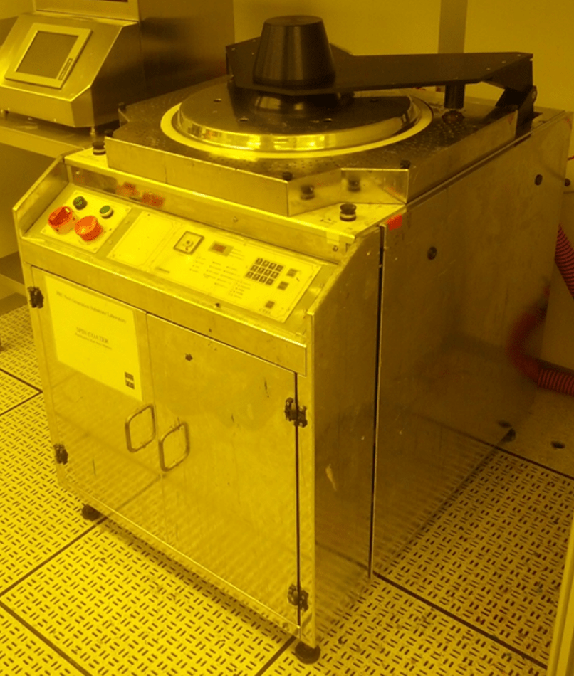
Spin-Coaters (Liquid Dielectric and Photoresists)

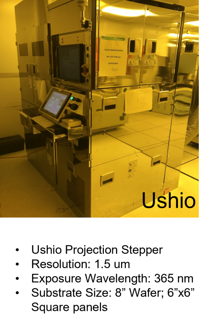
Photolithography Tools


Laser Microvia Fabrication Tools

Picosecond UV Laser (ESI Cornerstone)
- Picosecond 375 nm, UV Laser, …W Power
Machining head: Galvo scanner, fixed lens, cutting head, and Infinite Field of View (IFOV)
Max. Scanner field: 20×20 mm - Minimum Spot size: 6 µm for fixed head, 14µm for galvo head
XY stages travel: 300×300 mm
Submicron stages resolution
Femtosecond Near-IR Laser(Optec)
- Femtosecond 1030 nm, IR Laser, 4W Power
Machining head: Galvo scanner, fixed lens, cutting head, and Infinite Field of View (IFOV) Max. Scanner field: 20×20 mm - Minimum Spot size: 6 µm for fixed head, 14µm for galvo head
XY stages travel: 300×300 mm
Submicron stages resolution
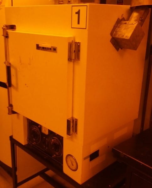
Curing Ovens